Microcircuit Photography

Background
This silicon zoo site has some interesting photos taken from under a microscope. They feature artwork added to commercial computer chips by circuit designers.
The Project
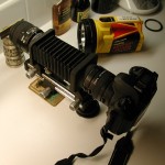
I was curious if it would be possible to capture micron-size features with my own digital camera, so I rigged my D100 camera with all the magnification gear I could find:
I ended up using three Kenko 12, 20 and 36mm extension stacked together, plus a set of old Nikon PB4 bellows, 60mm Micro Nikkor lense and a SunPak +4 magnifying lense.
The Subject

The subject is a computer chip which Chris Ematrudo and I designed for a college project. The chip is a systolic array processing element which the national science foundation paid to have fabricated. Unfortunately for the national science foundation, the chip didn’t work properly.
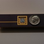
With the 60mm Micro Nikkor lense, you get an overview of the subject. The actual ‘chip’ is quite large because of the packaging used and the large number of pins required to address all the bits in the array processor.
Magnified and Photographed

The actual die containing the processor itself is only 1/16th of a square inch. The attached photo was taken using the 60mm Micro Nikkor plus 4+ magnifying filter.
To get additional magnification, I attached the PB4 bellows. The focal length is changed by twisting a thumb screw that pulls the front plane of the lense element along a metal track. Light metering, aperture, and shutter speed are adjusted manually with the bellows attached.
With the bellows fully extended, and all the components attached, very little visible light reaches the eyepiece. I had to turn all of the lights off in the room, cover subject with a sheet and use a bright flashlight to illuminate the circuit in order to see enough detail to properly focus.

The flashlight has to be carefully aligned to avoid creating a shadow from the lense on the circuit. The surface of the lense is just a few millimeters from the chip’s surface.
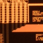
The text on the chip is not a functional piece of the electronics. It was created by depositing small squares of metal in a void on the silicon surface. The width of smallest features (including the traces which form the text) is 2 microns.
2 micron technology was nearly state of the art in 1992.
Ten years later, Intel’s Pentium III Xeon processor is fabricated using a 0.18-micron process.